

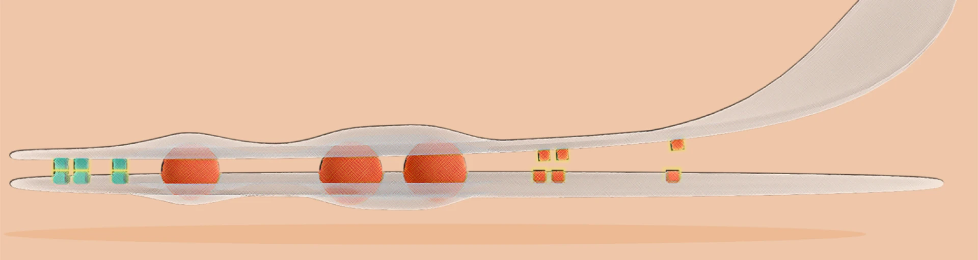
Defect Formation, Fusion and Stability in Scaled Wafer Bonding
In the DEFUSE project, the University of Twente and ASML will develop fundamental and technical knowledge on how such bonding defects form, grow and eventually lead to interface failure. The project studies three connected stages: 1) void formation by particle-surface interactions, 2) defect growth and fusion at bonded interfaces, and 3) the stability of downscaled Cu/liner/dielectric interfaces in hybrid bonding.
The results will provide experimentally supported defect thresholds, interface-stability limits and wafer bonding design guidelines. This understanding will help enable more reliable high-density wafer bonding for future semiconductor manufacturing and strengthens the Dutch knowledge base in chip technology, surface science and advanced metrology.