

Atomic-scale processing for Materials Innovation Driven by advanced Equipment
Objectives
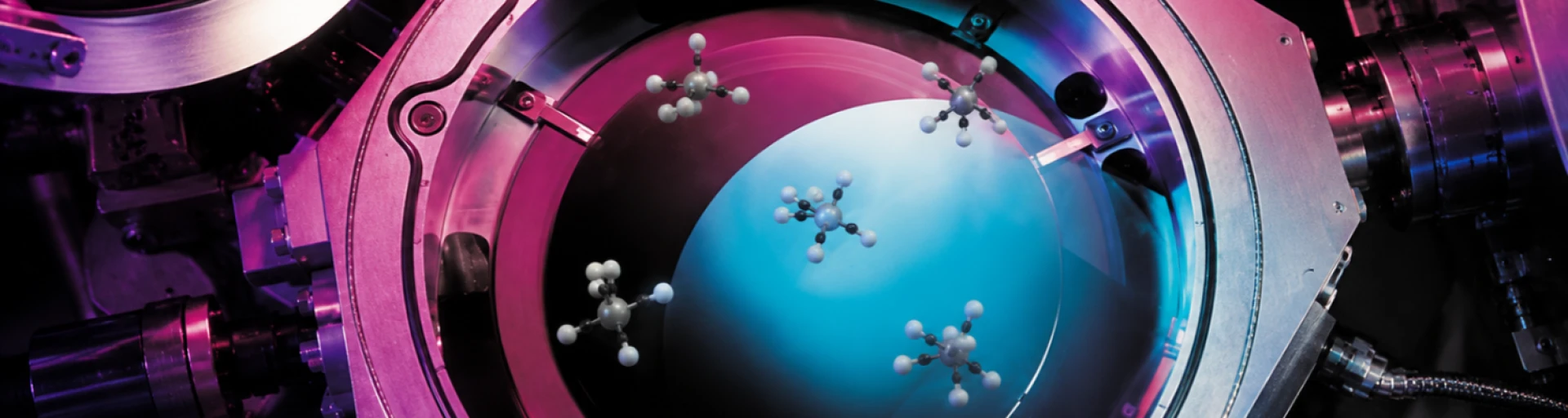
This project focuses on innovations in the field of semiconductor manufacturing equipment and develops new and improved processes for materials with atomic-scale accuracy. It combines advanced plasma diagnostics, surface chemistry, materials characterization and AI-assisted optimization to better understand and control the fundamental processes governing atomic layer deposition (ALD) and atomic layer etching (ALE). The research focuses on plasma surface interaction, selective etching, novel high-performance dielectric materials, and emerging two-dimensional semiconductor materials for future logic and memory chips.
Deliverables
The project will deliver predictive design rules and accelerated process development methodologies for semiconductor manufacturing equipment that strengthen the competitive position of the Dutch semiconductor industry.