

PHOMED
Photoacoustic overlay metrology for die-to-wafer bonding
In the semiconductor industry, it is essential to have measurement methods for the precise positioning of wafers prior to their processing. Preferably, optical methods are used because of their speed and non-invasive nature. However, in some cases, it is necessary to be able to measure through opaque materials. In this project, we are developing an optical concept to make such measurements possible.
Enabling optical measurements through optically opaque materials
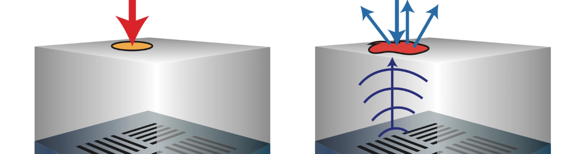
The ability to reliably make complex 3D integrated devices depends crucially on accurate metrology tools to guide the fabrication processes. This research proposal aims to develop such tools based on the concept of ultrafast-laser-driven photoacoustics. In semiconductor metrology, optical methods are preferred, but optically opaque materials are often encountered particularly in wafer-bonding applications. In photoacoustics, an ultrasound pulse is generated by rapid laser-induced local heating, which then interacts with the deeper layers where the metrology markers are located. The returning ultrasound is detected optically and the signal is processed to extract nanometer-level position information.