

New environmentally friendly generic approach for advanced die connection in Chip Packaging
Good contact and heat dissipation are crucial
In the field of power electronics, so-called wide-bandgap semiconductors such as SiC are rapidly gaining ground due to their superior performance compared to their traditional Si-based counterparts. The higher switching frequencies and power densities of these materials place high demands on the thermal management and mechanical reliability of the semiconductor chip and its package, especially because these chips are often used for critical applications under harsh conditions. For long-term optimal performance, the heat generated by the active part of the chip must be dissipated as efficiently as possible to the underlying substrate in the chip package.
Porous copper films as a solution
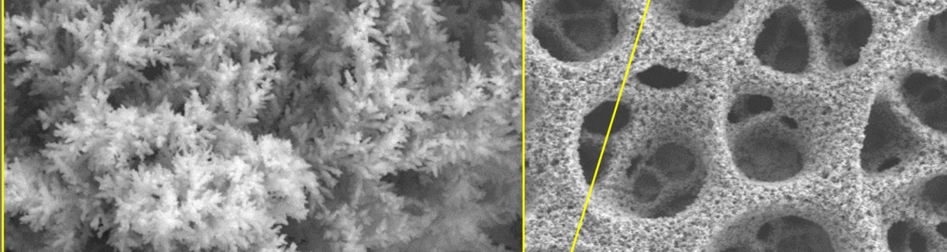
A recently developed process can produce nanostructured porous copper films using electrodeposition. Due to the rapid diffusion of material, these structures can achieve a very strong bonding between two elements. Smart Connect investigates which film structure achieves an optimal bonding and thermally conductive connection between a semiconductor chip and its underlying substrate. The goal is to develop an optimal generic interconnect technology for both the current generation of Si-based chips and for the emerging generation of chips based on heterogeneous engineered wafers.
Cooperation to reach the goal
In Smart Connect, a consortium consisting of Radboud University Nijmegen, TNO, and Coolsem Technologies is collaborating to develop an innovative chip interconnect technology. Radboud University is developing an innovative diffusion-driven chip interconnect method based on nano-textured porous copper films. Coolsem Technologies is developing Advanced Engineered Substrates (AES) on which the next generation of photonic, high-power, and high-frequency chips will be produced. Finally, TNO is developing the precise thermal measurement methods needed to monitor the progress made with the bonding technology and the AES, thus guiding the next steps in the research.